In the era of intelligent connectivity driven by 5G, AI, and the Internet of Things (IoT), the electronic manufacturing industry is undergoing an unprecedented transformation—products such as smartphones, automotive chips, and wearable devices are becoming increasingly miniaturized, integrated, and high-performance. Behind this evolution lies a critical challenge: how to efficiently and accurately handle electronic components that are shrinking to sizes as small as 0.4mm × 0.2mm (the 01005 package) and assemble them onto high-density PCBs (Printed Circuit Boards) with micron-level precision. Traditional manual or semi-automated loading methods, limited by human hand-eye coordination and fatigue, can no longer meet the demands of “high speed, high precision, and zero defects.”
Against this backdrop, the Automated Loading Assembly Machine for Electronic Components has emerged as a game-changer. This equipment integrates precision machinery, machine vision, robotic control, and data analytics to realize the full-process automation of “component feeding → posture correction → precision positioning → assembly bonding” for electronic components. It not only solves the pain points of manual operations but also becomes the core infrastructure for electronic manufacturers to achieve intelligent production, improve product quality, and reduce costs.
What Is an Automated Loading Assembly Machine for Electronic Components?
At its core, an Automated Loading Assembly Machine for Electronic Components is a specialized automation system designed to handle, position, and assemble electronic components (such as resistors, capacitors, IC chips, connectors, and sensors) onto target workpieces (e.g., PCBs, modules, or housings) without manual intervention. Unlike general-purpose assembly equipment, it is tailored to the unique characteristics of electronic components—including their small size, light weight, fragile structure, and diverse packaging forms (tape-and-reel, tray, tube, or wafer)—and focuses on three core requirements:
Precision: Assembly accuracy of ±0.005mm to ±0.02mm, matching the micron-level spacing of PCB pads.
Speed: Feeding and assembly rates of 1,000 to 50,000 components per hour, adapting to mass production beats.
Protection: Non-destructive handling of fragile components (e.g., thin IC chips, flexible connectors) to avoid damage from pressure or static electricity.
Typical application scenarios include SMT (Surface Mount Technology) lines, PCB module assembly, automotive electronic sensor installation, and medical device component bonding—covering almost all links in the electronic manufacturing value chain.
Core Technical Modules: How to Achieve “High Precision + High Efficiency”
The performance of an Automated Loading Assembly Machine for Electronic Components depends on the collaborative operation of five core technical modules. Each module addresses a key pain point in the electronic component loading and assembly process, forming a closed-loop system of “feeding-stabilization-positioning-assembly-inspection.”
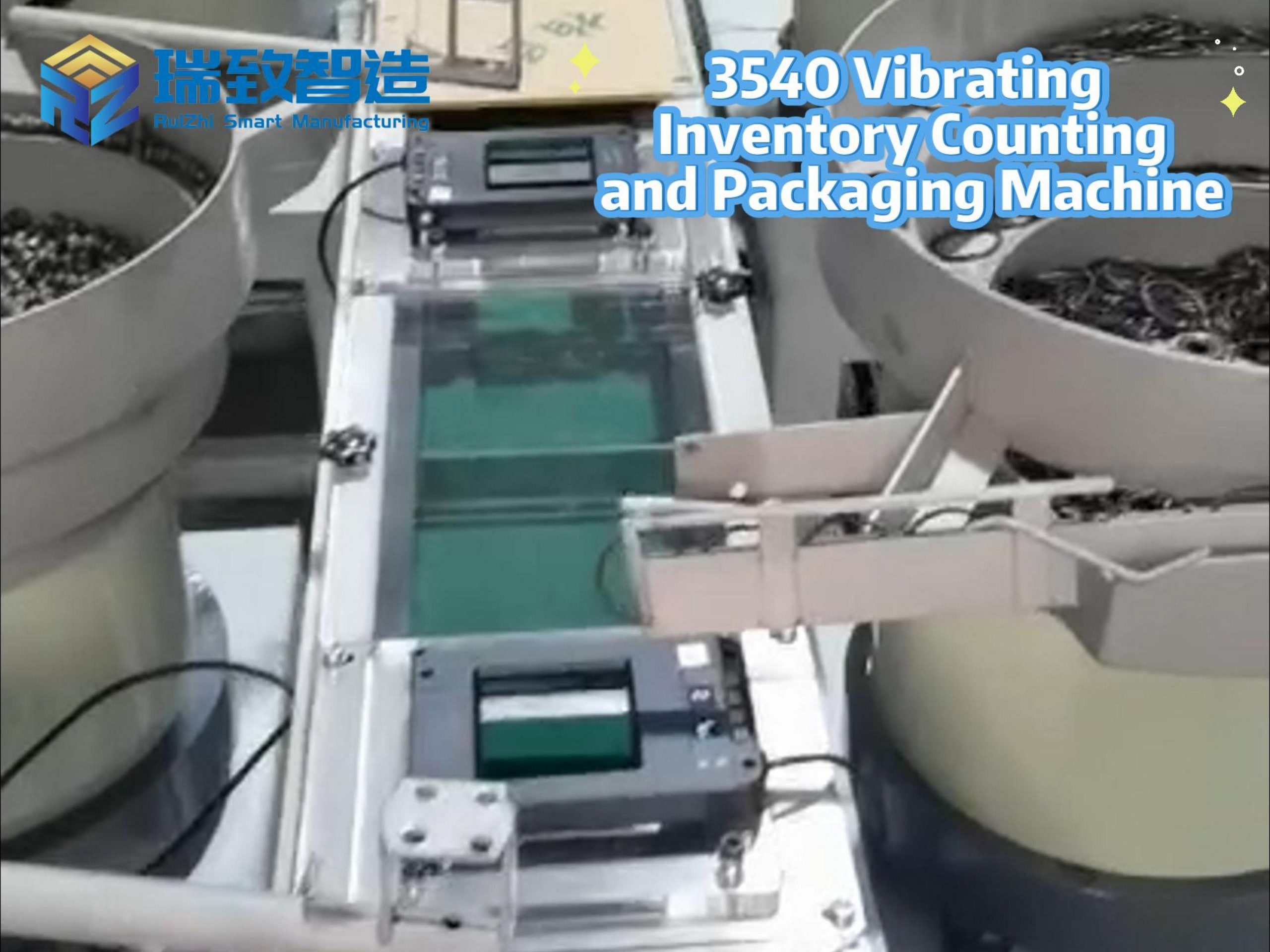
- Component Feeding System: Stable Supply for Diverse Packaging
The feeding system is the “starting point” of the assembly process, responsible for converting disorderly or packaged components into a uniform, transportable state. Given the diverse packaging forms of electronic components, the system adopts a modular design to adapt to different needs:
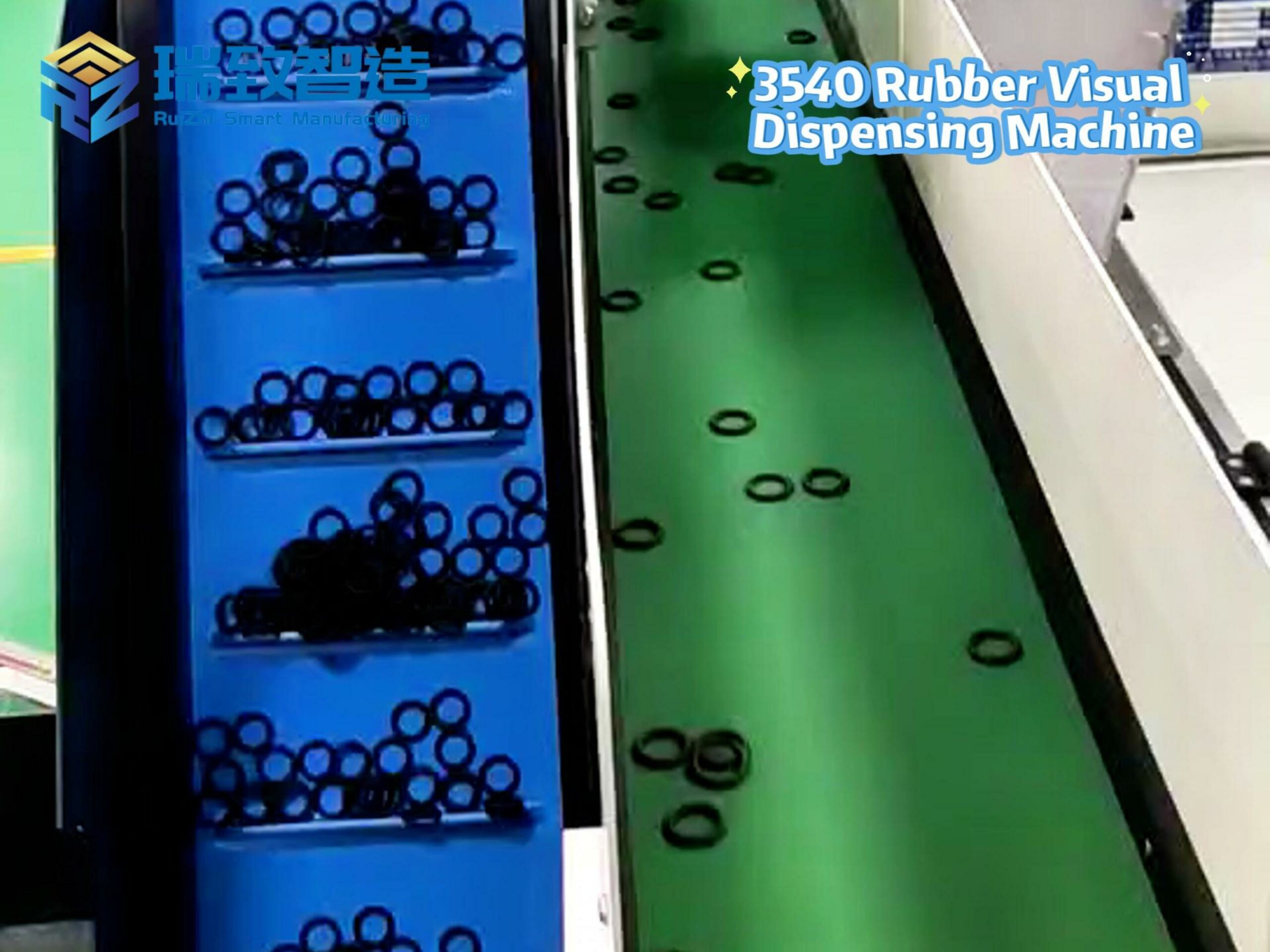
Tape-and-Reel Feeding (Most Widely Used):For components packaged in tape-and-reel (e.g., resistors, capacitors, small ICs), the system uses a reel feeder with a stepping motor to drive the tape forward at a fixed pitch. A precision needle or suction nozzle then peels off the top cover tape, exposing the components in the bottom tape pockets. The feeder can adjust the feeding speed in real time (100–500mm/s) according to the assembly beat, and supports quick reel replacement (within 30 seconds) for small-batch, multi-variety production. For example, in a smartphone SMT line, a tape-and-reel feeder can stably supply 01005 resistors at a rate of 3,000 pieces per hour, with a feeding success rate of over 99.95%.
Tray Feeding (For Large/Delicate Components):For large IC chips (e.g., CPU, GPU) or fragile components (e.g., image sensors), the system uses a tray handler with a robotic arm. The handler lifts the tray from a stack, transports it to a positioning platform, and uses a 2D vision camera to identify the position of each component in the tray. A vacuum suction nozzle then picks up the components one by one. To prevent static damage, the tray and suction nozzle are made of anti-static materials (e.g., carbon fiber-reinforced plastic), and the entire feeding process is carried out in an ESD (Electrostatic Discharge) protected area.
Wafer Feeding (For Bare Chips):In advanced semiconductor packaging (e.g., chiplet assembly), the system uses a wafer stage to handle bare chips. The stage rotates and moves precisely (with a positioning accuracy of ±0.001mm) to align the chip with the pick-up nozzle, while a laser thickness sensor detects the chip height to avoid collision. After picking up the chip, the system removes the protective film (if any) and transports it to the assembly station—critical for high-end applications such as AI accelerator chips.
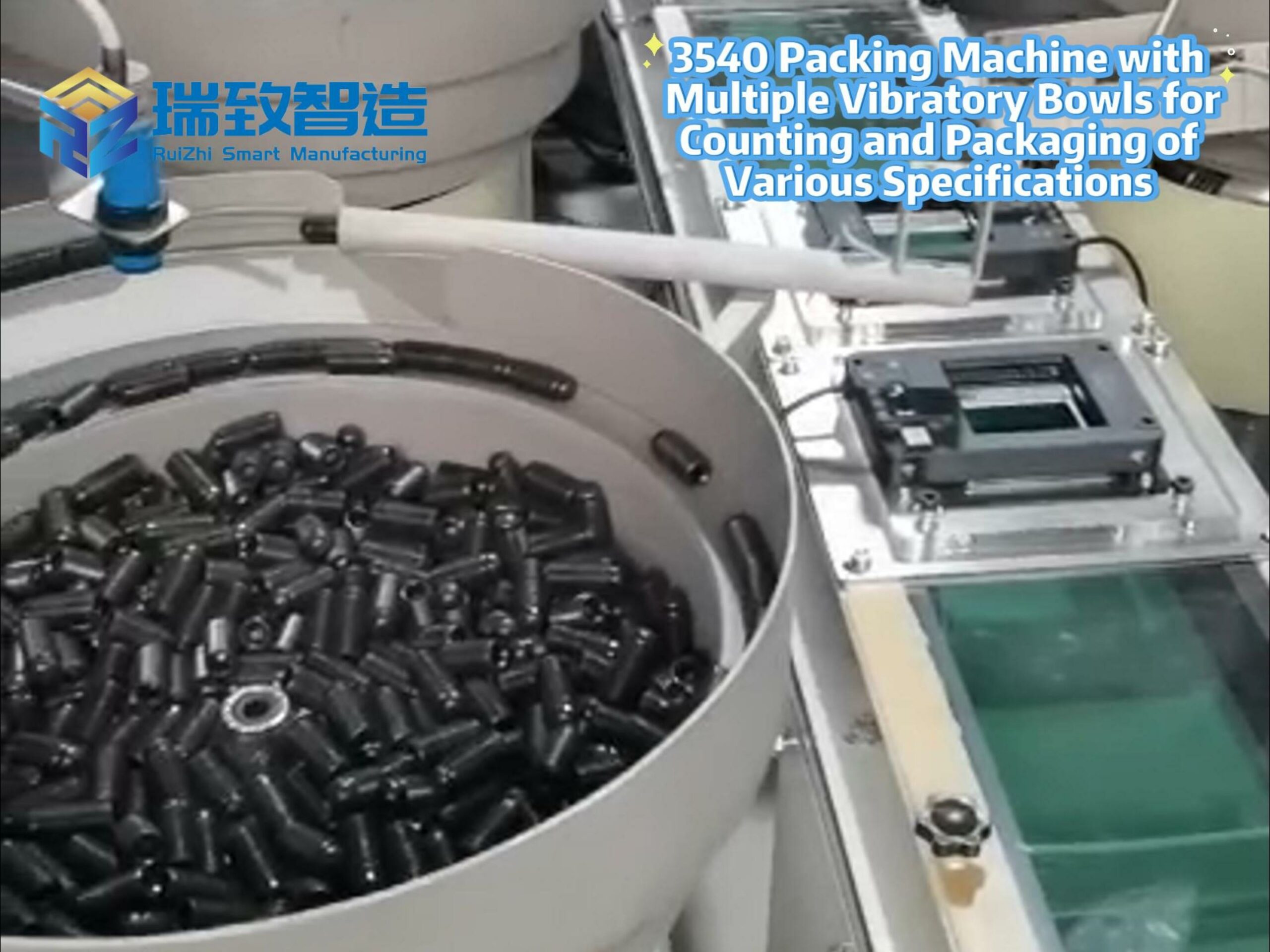
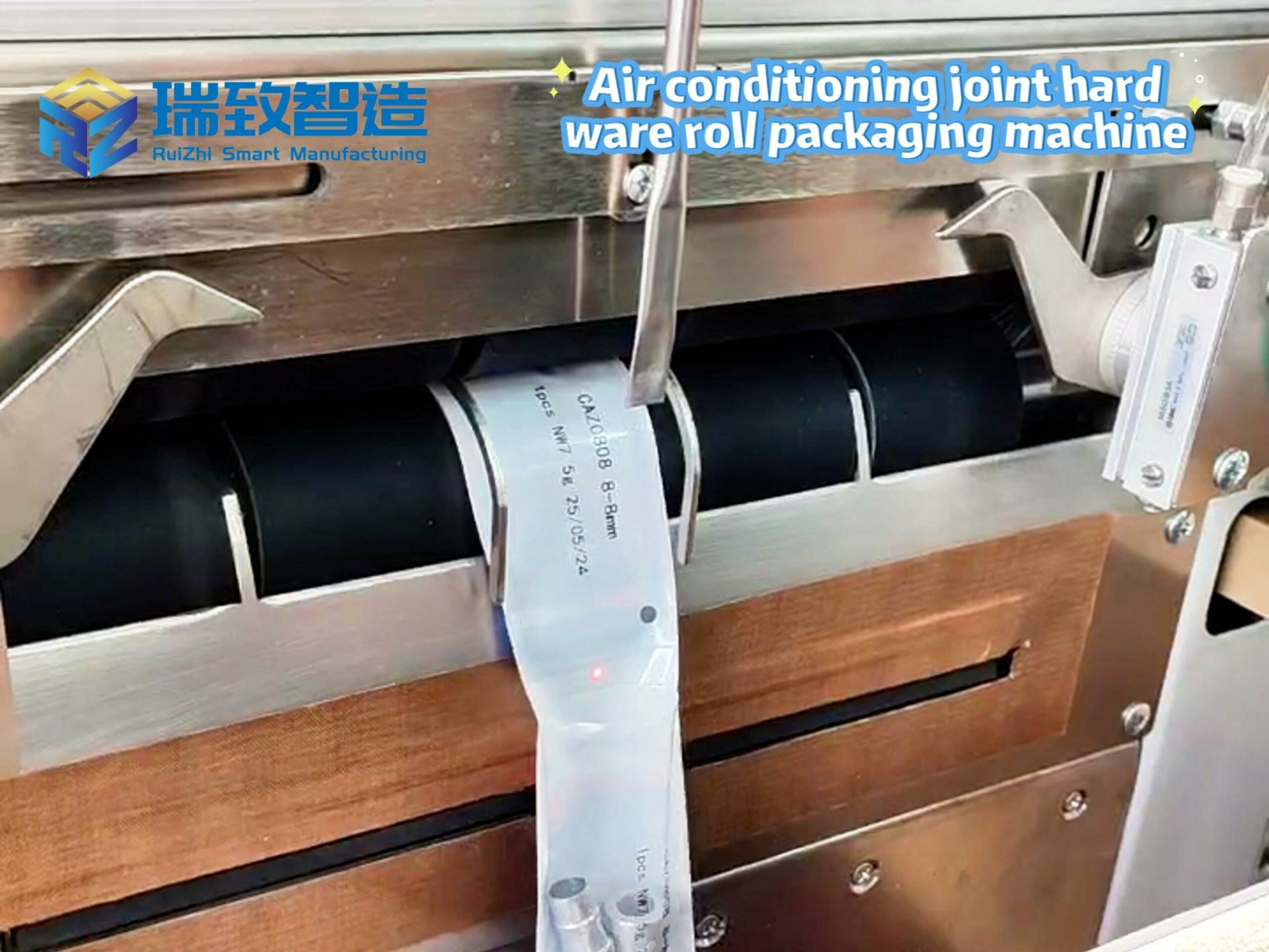
Tube Feeding (For Odd-Shape Components):For odd-shape components (e.g., connectors, inductors) packaged in plastic tubes, the system uses a vibratory tube feeder to drive components forward via low-amplitude vibration. A baffle at the tube outlet ensures components are oriented correctly (e.g., connector pins facing downward), and a fiber optic sensor verifies the posture before feeding. This method is widely used in automotive electronic assembly, where connectors need to be assembled with high consistency.
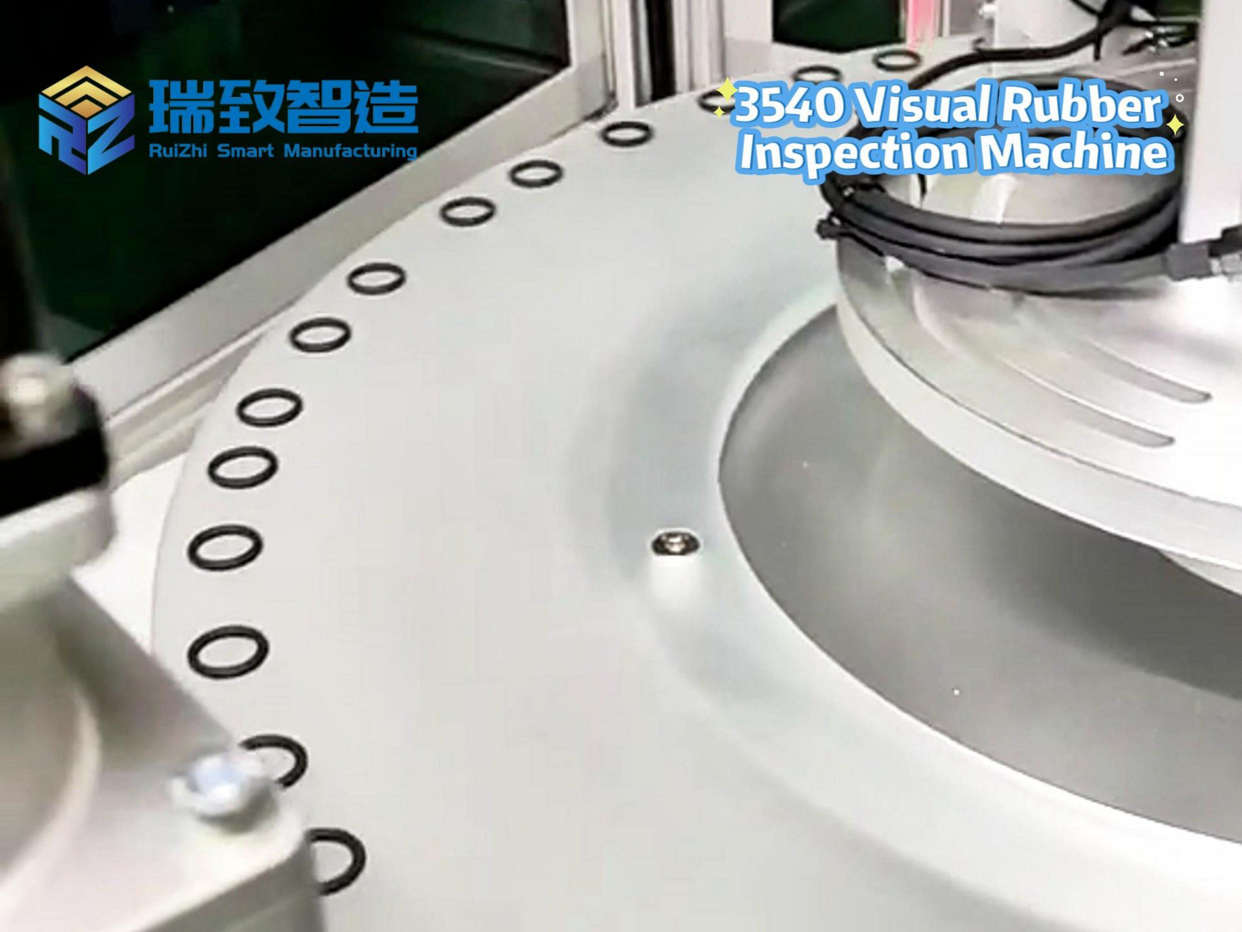
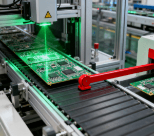
- Machine Vision Positioning System: The “Eyes” of Precision Assembly
Electronic components’ miniaturization and PCB pad density (up to 1,000 pads per square centimeter) require micron-level positioning accuracy—far beyond human visual capabilities. The machine vision system acts as the “eyes” of the machine, achieving real-time posture correction and precision alignment:
Dual-Camera Collaborative Positioning:Most high-end machines are equipped with two cameras: a component camera (installed above the feeding station) and a PCB camera (installed above the assembly station). The component camera captures the shape, size, and posture of the picked component (e.g., whether a resistor is tilted, whether an IC pin is bent), and calculates the offset (Δx, Δy, Δθ) relative to the ideal position. The PCB camera then captures the position of the target pad on the PCB, correcting for any PCB warpage or placement deviation. The control system integrates these two sets of data to adjust the robot’s movement trajectory, ensuring the component is placed exactly on the pad. For example, when assembling a 0.3mm-pitch IC chip, the dual-camera system can achieve a placement accuracy of ±0.008mm, reducing short-circuit risks caused by misalignment.
3D Vision for Complex Components:For components with irregular shapes or height differences (e.g., connectors with pins, sensors with lenses), 3D vision systems (using structured light or laser triangulation) are used to capture the component’s 3D profile. This helps avoid assembly errors caused by height mismatches—for instance, when assembling a automotive radar sensor, the 3D vision system detects the sensor’s lens height (±0.01mm) to ensure it is not pressed too hard, which could damage the optical components.
AI-Powered Defect Pre-Detection:Advanced vision systems integrate AI algorithms (e.g., deep learning) to pre-detect defective components during feeding. For example, the system can identify chips with cracked packaging, resistors with missing electrodes, or connectors with bent pins, and automatically reject them (via an air blow valve) before assembly. This reduces the post-assembly defect rate by 80% or more, avoiding costly rework on PCBs.
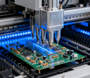
- Precision Assembly Execution Mechanism: The “Hands” of Stable Operation
The execution mechanism is responsible for physically moving the component from the feeding station to the PCB and completing the assembly (e.g., bonding, soldering, or pressing). To balance speed and precision, it typically uses high-performance robots and specialized end tools:
Delta Robots for High-Speed Assembly:In SMT lines or consumer electronics assembly (e.g., smartphone motherboards), delta robots are preferred for their ultra-high speed—they can achieve a maximum movement speed of 5m/s and a cycle time of less than 0.1 seconds per component. Equipped with a multi-nozzle head (4–12 nozzles), a single delta robot can assemble 10,000–30,000 small components (e.g., 01005 resistors) per hour. The robot’s lightweight design and parallel kinematics structure ensure minimal vibration, maintaining a repeated positioning accuracy of ±0.01mm.
SCARA Robots for Medium-Precision Tasks:For components that require horizontal movement and rotation (e.g., connectors, inductors), SCARA robots are used. Their arm structure allows for precise horizontal positioning (±0.005mm) and rotation (±0.01°), making them ideal for assembling components with directional requirements (e.g., a USB connector that must align with the PCB’s notch). SCARA robots are widely used in automotive electronic module assembly, where they can complete 2,000–5,000 assembly tasks per hour.
End Tools: Non-Destructive Handling:The end tool (e.g., vacuum suction nozzle, mechanical gripper) is critical for protecting fragile components. Vacuum suction nozzles are used for most small components—they are made of soft, anti-static silicone or rubber, and the suction force is adjustable (0.1–5N) according to the component’s weight (e.g., 0.1N for a 01005 resistor, 3N for a large IC). For components that cannot be sucked (e.g., connectors with irregular surfaces), mechanical grippers with force sensors are used to adjust the clamping force in real time, avoiding pin deformation.
- Process Integration Module: Beyond Loading—One-Stop Assembly
Modern Automated Loading Assembly Machines are no longer limited to “loading + placing”—they integrate downstream processes (e.g., soldering, bonding, curing) to form a one-stop assembly line, reducing production steps and improving efficiency:
In-Line Soldering:Some machines integrate laser soldering or hot-air soldering modules. After placing the component on the PCB pad (coated with solder paste), the laser soldering head heats the pad to 220–250°C (for lead-free solder) in 0.5 seconds, melting the solder and bonding the component. This is widely used in high-reliability applications such as medical device PCBs, where solder joint quality directly affects device safety.
Adhesive Bonding:For components that do not require soldering (e.g., flexible connectors, sensors), the machine integrates a dispensing module to apply UV-curable adhesive to the PCB pad. After placing the component, a UV lamp cures the adhesive in 2–5 seconds, ensuring a stable bond. This method avoids thermal damage to heat-sensitive components (e.g., OLED display drivers).
Press-Fit Assembly:For power components (e.g., MOSFETs, capacitors) that require tight mechanical contact, the machine uses a precision press-fit module with force control. The press applies a fixed force (5–50N, adjustable via a load cell) to press the component into the PCB socket, ensuring good electrical contact without damaging the component or socket. This is common in industrial electronic equipment (e.g., inverters) where high current flow requires reliable connections.
- Quality Inspection and Data Traceability: Ensuring “Zero Defects”
In electronic manufacturing, “zero defects” is not just a goal—it is a requirement, especially for automotive and medical electronics. The quality inspection and traceability module ensures that every assembly step is monitored and recorded:
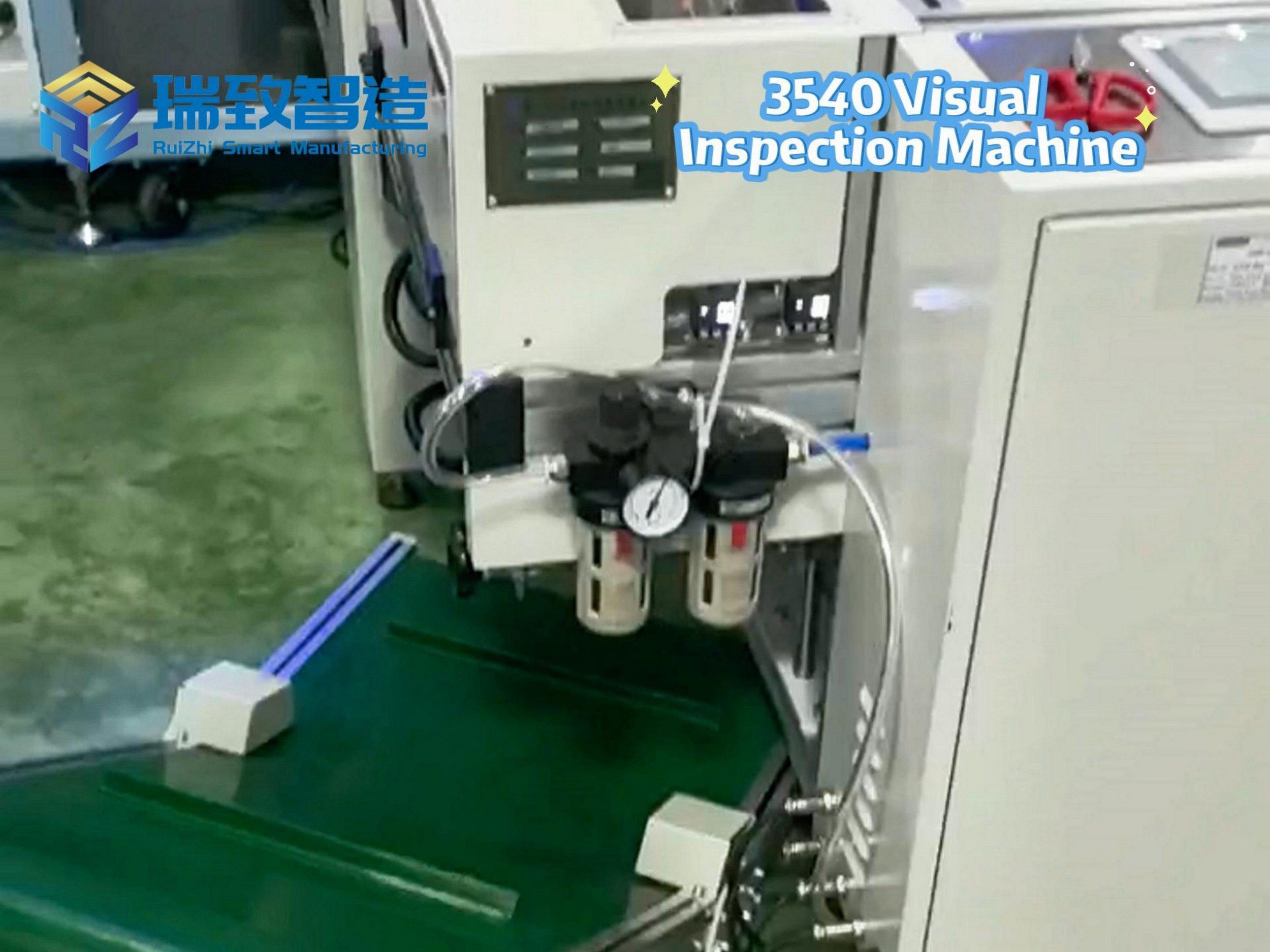
Online Visual Inspection (OLVI):After assembly, a high-resolution camera (12–24 million pixels) captures images of the assembled components to check for defects such as missing components, offset placement, solder bridges (short circuits), or tombstoning (components standing upright). The system compares the images to a “golden sample” and automatically flags non-conforming products, which are then diverted to a rework station.
Electrical Test Integration:Some advanced machines integrate in-circuit testing (ICT) or functional testing (FCT) modules. After assembly, the PCB is connected to test probes to check for electrical continuity, short circuits, or component functionality (e.g., whether a resistor’s resistance value is within the specified range). This catches defects that visual inspection cannot, such as faulty components or poor solder joints.
Full-Lifecycle Data Traceability:The machine is connected to the factory’s MES (Manufacturing Execution System) via industrial Ethernet. Every assembly step—including component batch numbers, feeding time, assembly parameters (e.g., suction force, soldering temperature), and inspection results—is recorded in a database. If a quality issue is found later (e.g., a batch of defective resistors), manufacturers can quickly trace which PCBs used those resistors and recall them, minimizing losses. This meets industry standards such as IPC-A-610 (for electronic assembly) and ISO 13485 (for medical devices).
Industry Applications: Tailored Solutions for Diverse Needs
The Automated Loading Assembly Machine for Electronic Components is not a “one-size-fits-all” device—it is customized to meet the unique requirements of different electronic manufacturing sectors. Below are its key applications:
- Consumer Electronics: Chasing “Miniaturization + High Speed”
In the consumer electronics industry (smartphones, laptops, wearables), components are becoming increasingly miniaturized (e.g., 008004 packages, 0.25mm-pitch ICs), and production beats are extremely tight (a smartphone factory may produce 100,000 units per day). Automated loading assembly machines here focus on speed and precision:
Smartphone PCB Assembly: A delta robot-equipped machine assembles 30,000+ 01005 resistors/capacitors per hour onto a smartphone motherboard, with a placement accuracy of ±0.008mm. The machine also integrates UV bonding for flexible connectors (e.g., screen connectors), ensuring they withstand repeated bending.
Wearable Device Assembly: For devices like smartwatches, which have smaller PCBs and more fragile components (e.g., OLED drivers), the machine uses 3D vision to avoid component damage and a low-force press-fit module to assemble small batteries, reducing the defect rate to less than 0.1%.
- Automotive Electronics: Prioritizing “Reliability + Durability”
Automotive electronics (e.g., ADAS sensors, in-vehicle infotainment systems) require components to withstand extreme temperatures (-40°C to 125°C) and vibrations, so assembly reliability is critical. Machines here focus on robust processes and strict testing:
ADAS Sensor Assembly: A SCARA robot assembles a lidar sensor onto a PCB, using 3D vision to align the sensor’s lens with the PCB’s optical window (accuracy ±0.01mm). After assembly, the machine performs a functional test to verify the sensor’s distance measurement accuracy, ensuring it meets automotive safety standards (e.g., ISO 26262).
Battery Management System (BMS) Assembly: BMS PCBs use high-power components (e.g., shunt resistors, MOSFETs) that require press-fit assembly. The machine applies a controlled force (20–30N) to press the components into the PCB, and an ICT test checks for electrical continuity, ensuring the BMS can safely monitor battery performance.
- Medical Electronics: Meeting “Sterility + Traceability”
Medical devices (e.g., glucose monitors, ECG machines) have strict requirements for sterility, biocompatibility, and traceability. Machines here are designed for cleanroom operation and full data recording:
Glucose Monitor PCB Assembly: The machine operates in a Class 100,000 cleanroom, using anti-static materials and HEPA filters to prevent dust contamination. After assembling the PCB, the machine performs a functional test to ensure the monitor can accurately measure glucose levels, and records the component batch numbers and test results for FDA/CE compliance.
Implantable Device Assembly: For small implantable devices (e.g., pacemakers), the machine uses a micro-robot with a vacuum suction nozzle (0.1mm diameter) to assemble tiny components (e.g., 0.5mm × 0.5mm IC chips). The entire process is monitored by a 24-megapixel camera to ensure no defects, as even a small error could endanger the patient.
- Industrial Electronics: Balancing “Flexibility + Cost”
Industrial electronics (e.g., PLCs, frequency converters) often require small-batch, multi-variety production, so machines here focus on flexibility and quick changeover:
PLC Module Assembly: The machine uses a modular feeder system that can switch between different component types (e.g., relays, capacitors, connectors) in 5–10 minutes. A collaborative robot works alongside human operators to handle complex assembly tasks (e.g., wiring terminals), reducing changeover time by 60% compared to traditional machines.
Frequency Converter Assembly: The machine integrates a press-fit module for power IGBTs (Insulated Gate Bipolar Transistors) and an electrical test module to check the converter’s output voltage and current. This ensures the converter can withstand high loads in industrial environments, while the machine’s data traceability function helps with maintenance and troubleshooting.
Current Challenges and Future Trends
While Automated Loading Assembly Machines have become mainstream in electronic manufacturing, they still face challenges that drive continuous innovation:
- Current Challenges
Ultra-Miniaturization Limits: Components like 008004 packages (0.2mm × 0.1mm) are approaching the physical limits of handling—vacuum suction nozzles may struggle to grip them stably, and vision systems may have difficulty distinguishing their postures.
High Cost Barriers: A high-end machine for semiconductor packaging can cost $1–5 million, making it unaffordable for small and medium-sized enterprises (SMEs).
Complex Component Handling: Odd-shape components (e.g., flexible PCBs, MEMS sensors) require customized feeding and assembly solutions, increasing the machine’s complexity and cost.
- Future Trends
AI-Driven Intelligent Optimization: AI will be used to optimize feeding speeds, assembly paths, and maintenance schedules. For example, an AI algorithm can analyze historical data to predict when a feeder will fail, enabling preventive maintenance and reducing downtime by 40%.
Digital Twin Virtual Debugging: Manufacturers will use digital twins to simulate the machine’s operation in a virtual environment before on-site deployment. This allows for debugging of programs, collision detection, and process optimization, cutting on-site setup time by 50%.
Modular and Low-Cost Designs: To meet SME needs, machine manufacturers will develop modular systems—users can start with a basic feeding module and add vision or assembly modules as needed, reducing initial investment by 30–50%.
Green and Low-Energy Operation: New machines will use energy-saving motors, LED lighting, and heat recovery systems to reduce energy consumption by 20–30%, aligning with global carbon neutrality goals.
Human-Machine Collaboration (HRC): Collaborative robots will be more widely used, allowing workers to handle complex tasks (e.g., component inspection) while the machine handles repetitive loading and assembly. Safety sensors will ensure workers and robots can operate side-by-side without risk.
Conclusion
The Automated Loading Assembly Machine for Electronic Components is not just a tool for replacing manual labor—it is the backbone of modern electronic manufacturing. As electronic products become more miniaturized, integrated, and high-reliability, the machine’s role in ensuring precision, efficiency, and quality will only grow. From consumer electronics to automotive and medical devices, it is the invisible force driving innovation in the electronics industry.
In the future, with the integration of AI, digital twin, and modular technologies, these machines will become more intelligent, flexible, and affordable—enabling not just large enterprises but also SMEs to embrace high-precision electronic manufacturing. For the global electronic industry, the Automated Loading Assembly Machine is more than a piece of equipment; it is a key enabler of the “smart manufacturing revolution,” paving the way for a new era of electronic products that are smaller, faster, and more reliable.